Black Pad Phenomenon: A Hidden Threat to PCB ReliabilityAuthor : Iris solder paste no clean September 23, 2025Table of ContentsIf you've ever encountered PCB failures—like intermittent connections, weak solder joints, or even total circuit failure—chances are you've come across the notorious Black Pad Phenomenon. This defect, most commonly associated with ENIG (Electroless Nickel Immersion Gold) surface finishes, can lead to costly rework, field returns, and compromised product reliability. In this article, we'll explain what the black pad defect is, its root causes, its damaging effects, and—most importantly—how partnering with a manufacturer with rigorous process controls, like ALLPCB, can help you prevent it.
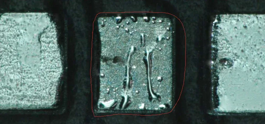
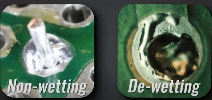
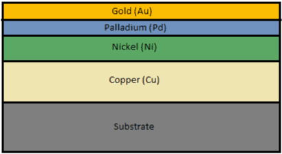
What Is the Black Pad Defect?The black pad defect is a solderability failure mode in PCB manufacturing that results in a non-wettable, dark-colored pad surface. Instead of exhibiting the typical bright gold appearance expected of ENIG, affected pads appear dull, grainy, or even black.
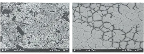
Microscopically, this darkened surface is a phosphorus-rich, brittle layer that forms in the nickel during the ENIG process. IPC-4552 (the industry specification for ENIG) defines this as nickel corrosion and classifies it into levels based on severity and depth. Under 1000× magnification, corrosion manifests as 'spikes,' 'spreader spikes,' or a 'black band' at the nickel–gold interface. Level-3 corrosion, as defined by IPC-4552A, is considered rejectable for Class 3 high-reliability products.
This corrosion prevents proper metallurgical bonding during soldering, leading to:
Consequences for PCB Performance and ReliabilityThe impact of black pad goes beyond assembly challenges—it affects the electrical and mechanical reliability of the entire product. Electrical & Functional Impacts
Assembly & Mechanical Risks
These risks are critical for automotive, aerospace, and medical electronics, where reliability is non-negotiable.
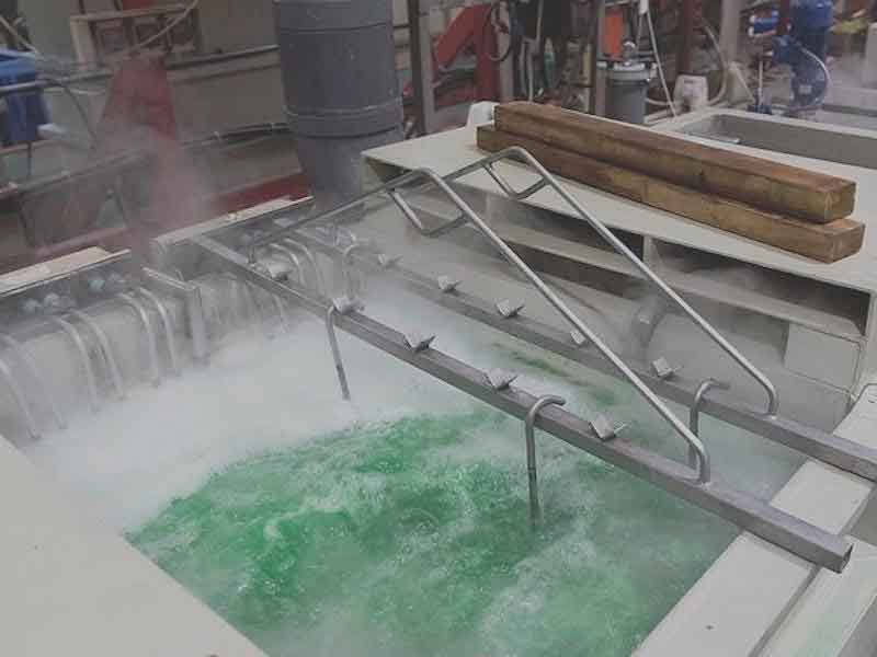
Why Black Pad HappensThe phenomenon is primarily linked to nickel over-corrosion during ENIG plating. Key contributing factors include:
IPC Requirements: What the Standards SayIPC-4552B sets the following key parameters for ENIG finish:
By adhering to these process windows, manufacturers can dramatically reduce the risk of black pad formation.
How ALLPCB Prevents Black Pad DefectsAt ALLPCB, we take a process-control-first approach to ENIG plating. Our quality system is aligned with IPC-4552B guidelines and includes: Electroless Nickel Process Control
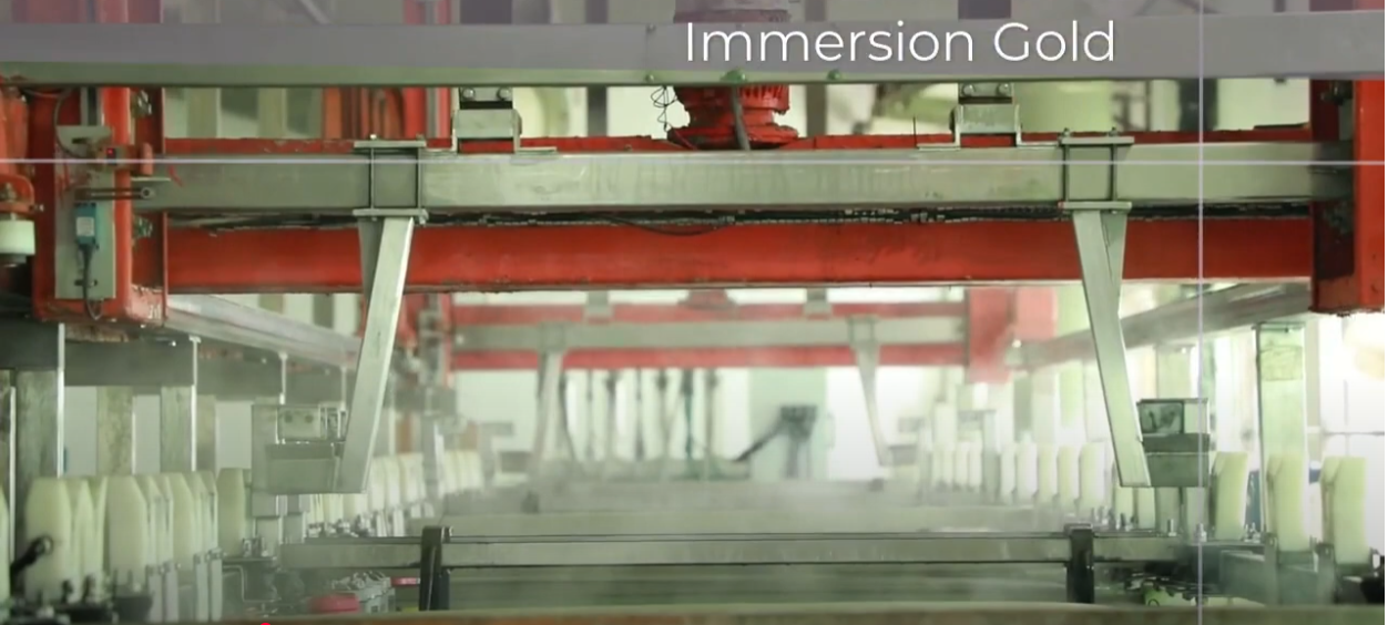
Immersion Gold Process Optimization
Comprehensive Chemical Management
Tips for Designers & Buyers to Reduce RiskWhile process control is the manufacturer's responsibility, design and sourcing choices matter too:
ConclusionBlack pad is a well-known but avoidable defect. By understanding its causes and aligning with IPC-4552B process controls, you can minimize risk and ensure long-term product reliability. At ALLPCB, we combine real-time process monitoring, predictive analytics, and strict quality control to deliver ENIG finishes with outstanding solderability and reliability—helping you build products that perform flawlessly in the field. Share · · · · The Role of Flux in PCB Wave Soldering: Selection, Application, and Residue RemovalMarch 16, 2026PCB wave soldering flux types include rosin, water-soluble, and no-clean options with varying activity levels for oxide removal and solder flow. This guide covers selection criteria, spray foam drop-jet application methods, residue removal processes, and alternatives like nitrogen blanketing to boost joint reliability and yields for engineers. Article Achieving Uniform Solder Fillets in PCB Wave Soldering: Process ControlMarch 16, 2026Achieve uniform solder fillets in PCB wave soldering with process control strategies. Optimize flux, preheat, wave height, conveyor speed for consistent fillet shape, height, and wetting balance. Includes visual inspection tips and troubleshooting for reliable through-hole assemblies. Boost quality in production. Article Optimizing Conveyor Speed for Efficient PCB Wave SolderingMarch 16, 2026Learn PCB wave soldering conveyor speed calculation to manage dwell time, immersion depth, and throughput effectively. Electric engineers get practical steps, best practices, and troubleshooting tips for higher process efficiency and fewer defects in wave soldering operations. Article Understanding IPC Standards for PCB Surface Finishes: Ensuring Quality and ComplianceMarch 11, 2026Understand IPC standards IPC 4552 ENIG and IPC 4553 immersion silver for PCB surface finishes. Ensure compliance, enhance solderability, and prevent common defects to achieve reliable, high quality circuit boards. Article High Speed Routing Techniques: PCBMarch 11, 2026Master high speed routing in PCBs to ensure signal integrity and minimize electromagnetic interference. Learn essential techniques for robust designs, from controlled impedance to differential pair strategies. Prevent performance issues and achieve reliable electronics. Article Miniaturization Challenges in PCB AssemblyMarch 11, 2026Navigate the complexities of high density interconnect PCB assembly and precise component placement. Learn to tackle miniaturization challenges, from tiny part handling to thermal stress, ensuring robust and reliable electronics. ArticleGet Instant PCB |